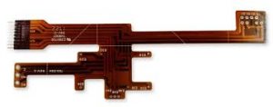
High-Density Routing in Flexible PCBs
Using flexible PCBs in your design provides an array of advantages including a reduction in part size and weight, the ability to route in tight spaces, and the option to accommodate a wider range of component lead pitches. However, there are a number of important considerations that must be made to ensure that your board will meet both your electrical and mechanical requirements. The most critical factor in this regard is the stack-up. This is because the stack-up determines how much space there will be for traces and components as well as the impedance requirements.
The best way to ensure that the stack-up will allow for high-density routing is to meet with your preferred fabricator before starting the design process. They will be able to advise you on what can and cannot be achieved with a given fabrication technology, and can offer suggestions for improving your design to achieve the necessary impedance.
When creating your flexible pcb board stack-up, try to avoid using too many layers. This will reduce the amount of copper that can be etched and will make it more difficult for you to place your traces and components. In addition, you will need to make sure that you have enough layer thicknesses in order to accommodate the appropriate via density and the Impedance requirements.

How to Achieve High-Density Routing in Flexible PCBs
Another important aspect of the stack-up is to minimize the use of vias where possible. This will allow you to maximize the surface area of your traces, and also help you to reduce noise due to cross-talk between adjacent traces. The best way to do this is to replace standard through-hole vias with blind or buried vias, or even better, to use microvias that are only used on signal layers. This will eliminate the need to drill through the entire stack-up and will save you considerable cost as a result.
It is also important to consider the effect that bending will have on your circuit. When a copper trace is bent, stress and cracks can develop that will negatively impact its performance. To avoid this, you should always keep in mind the maximum allowable bending radius for the flex section of your PCB. It is also recommended to use curved rather than straight traces whenever possible, and to provide ample bend relief in your layout.
For the plated through-holes and vias on your flex PCB, be sure to use teardrop (pad fillet) shaped connections to prevent stress concentration points. You should also give your annular rings the biggest possible diameter, as this will increase the strength of the connection between the ring and the connected copper traces. Additionally, you should always use a rounded corner for any cutouts or slits on your flex PCB to decrease the likelihood of them tearing or ripping during assembly and production. This will also aid in the longevity of your flex PCB.